This blog will show a way on how you can have reusable PCB design blocks in KiCAD V9. This workaround can be used with the new Multi-Channel feature or plugins like Replicate Layout.
This guide uses KiCAD Version: 9.0.3-9.0.3-0~ubuntu24.04.1, release build.
Step 1 – Setup: Your Library
In this step we setup our library file. The library file is a normal KiCAD project we have saved in a shared location.
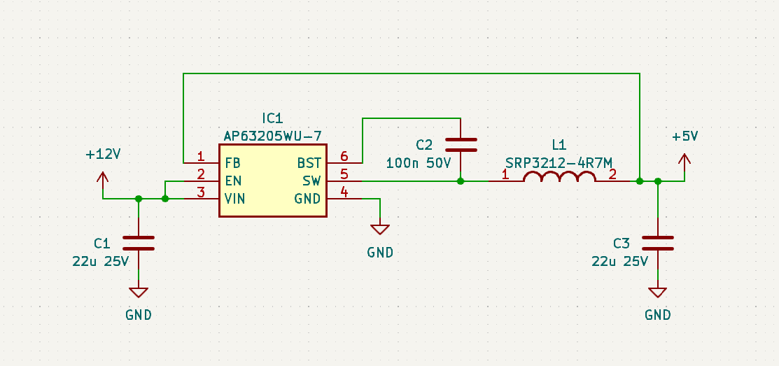
First step is to create your circuit as one usually does. Note here, that this is just a simplified example, so don’t go and copy it 🙂
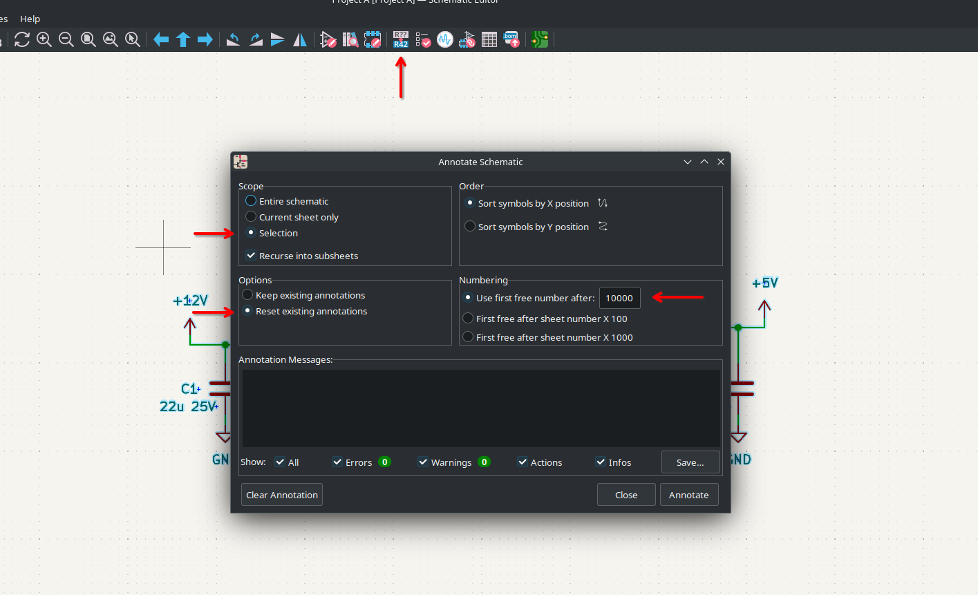
After creating your circuit you have to change the default annotation. This step is required for the PCB copy to work! To do this select your design block and open the Annotate Schematic tool. Change the Scope, Options and Numbering as seen in the image above. You can also select a different starting index, we just use a round number that is above the expected numbers we usually find in our designs.
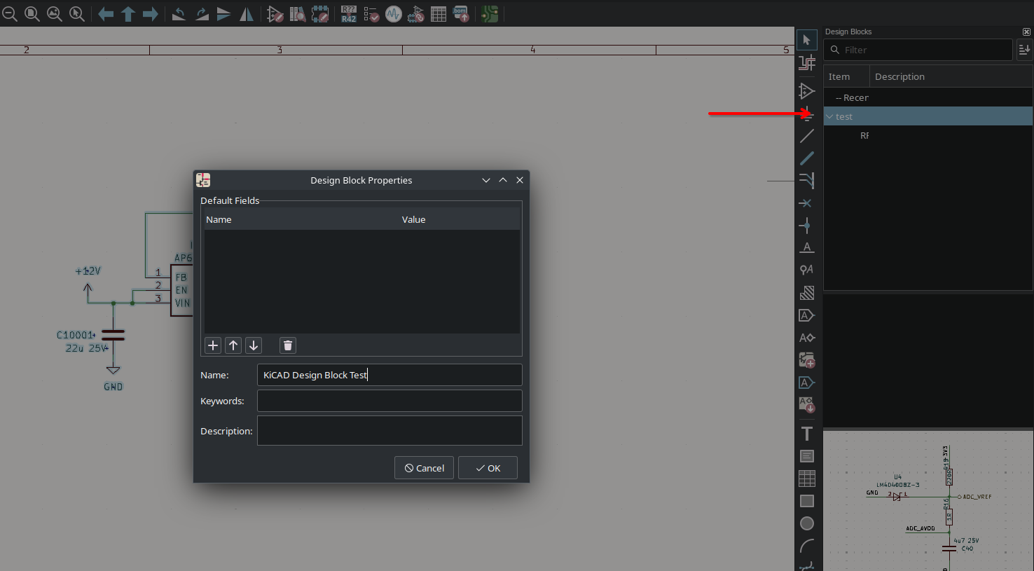
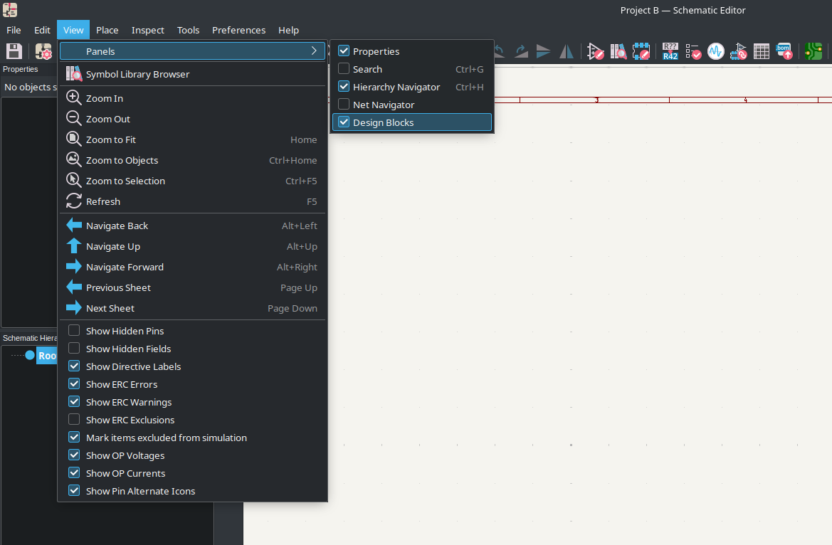
After completing your schematic save it as a design block. This can be done by selecting your circuit, right clicking your library and selecting Save Selection as Design Block …. More details on how they can be created are in the KiCAD Documentation. If your Design Blocks panel is hidden you can reveal it by going to View > Panels > Design Blocks.
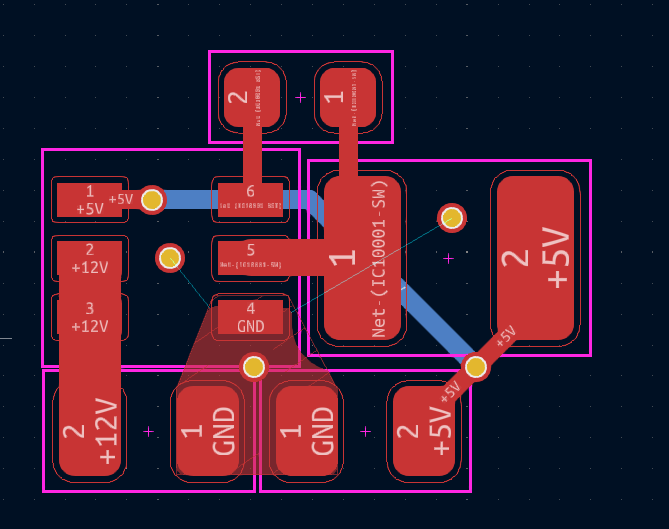
Now you can build your PCB as usual. If you want reference designators in your final design you can position them as well. I have hid them in this example. Your final designator number will be a lot smaller than the one you see now. If you don’t change the alignment of the designator text they usually shrink symmetrically around their center.
Step 2 – Adding it to a new schematic
In this Step we add a created design block to a new project and copy over the PCB section of it.
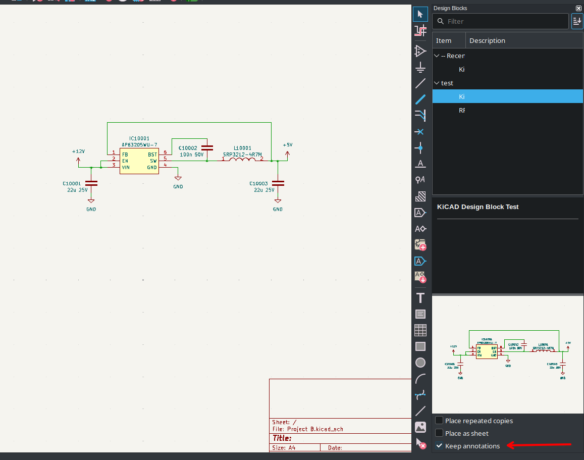
Add your design block from Step 1 into your new project with Keep annotations enabled as shown in the figure above.
Open the PCB of your new project, do not press Update PCB from Schematic … or any re-annotation button!
Open the PCB of your library project in a second window and copy the PCB section of your design block (select PCB items you want to copy and use the normal STRG-C or Right Click > Copy).
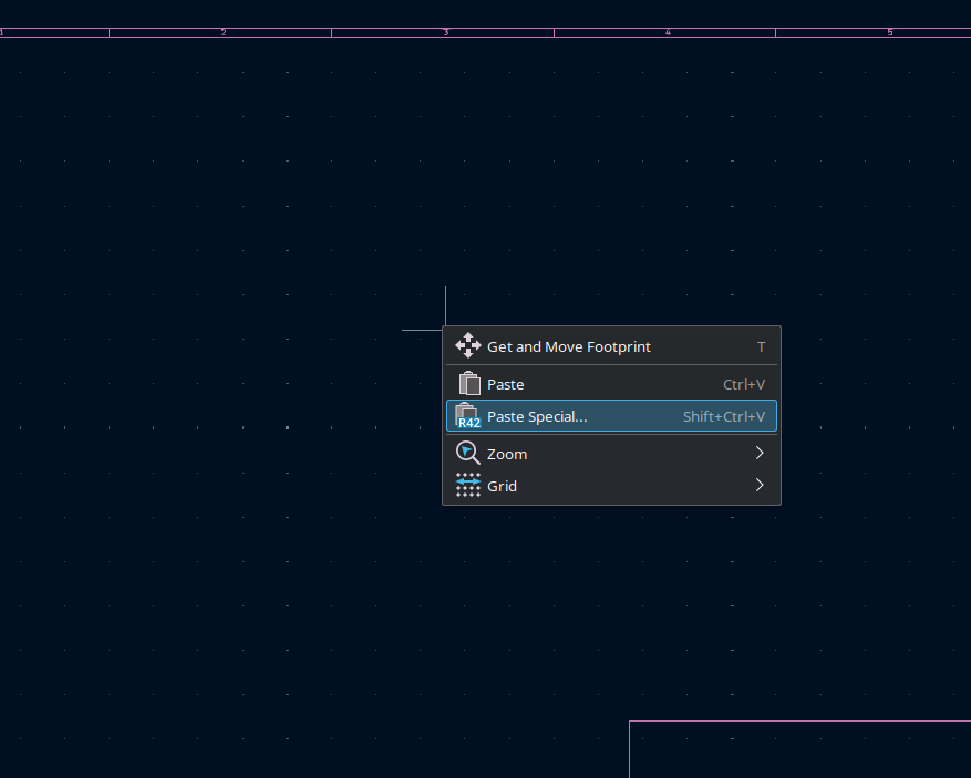
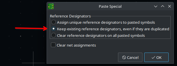
Go back to your new project and press the Right Click > Paste Special … as shown above. This will open a Paste Special window, select Keep existing reference designators, even if they are duplicated as shown below. (Note: this will not work if you have multiple parts with the same reference designators. If you want to add multiple design blocks see Step 3)
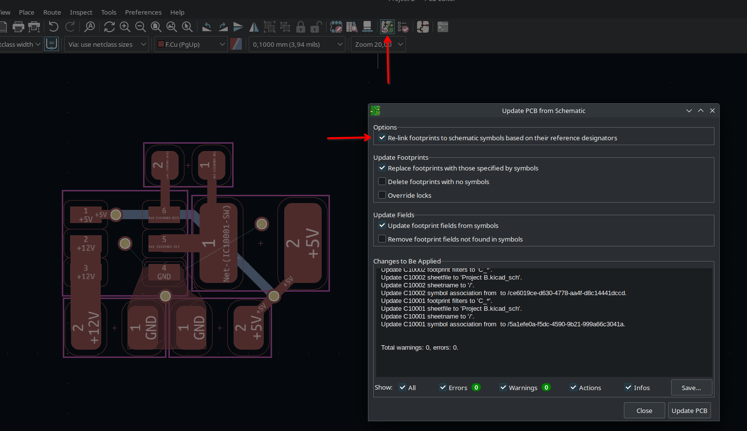
We now have to re-link the pasted footprints back to their symbols. To do this open the Update PCB from Schematic window, enable Re-link footprints to schematic symbols based on their reference designators, and press Update PCB. As the name states this will re-link the parts by the reference and is the reason for the importance of keeping the reference designation and the work around that.
To confirm that the pasted parts are linked with the schematic parts you can select one of the parts on the PCB and see if the correct schematic part is highlighted.
Step 3 – Cleaning up the designators
This step is optional if you just add one instance of the block or don’t care about the reference designator indices.
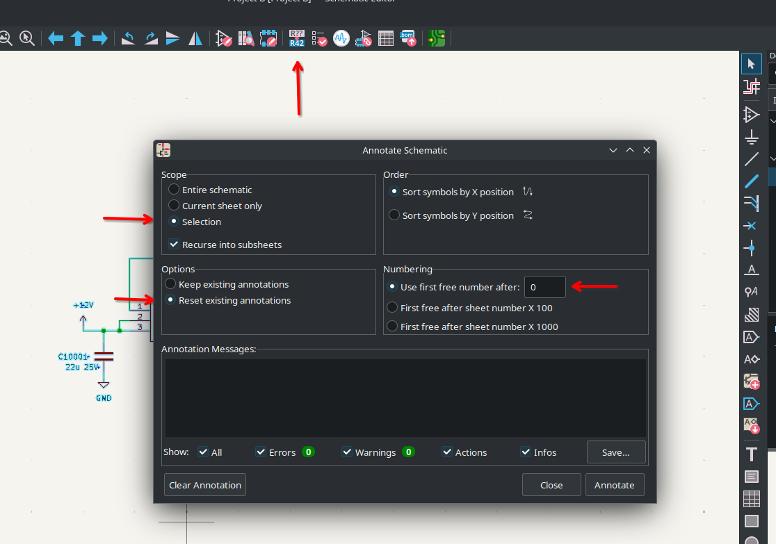
To update the designators you again have to select your design block and open the Annotate Schematic tool. Change the Scope, Options and Numbering as seen in the image above. This time we just reset the number 0 to follow the PCBs annotation.
After re-annotating the block you have to go back to the PCB and update it. This time disable the Re-link footprints to schematic symbols based on their reference designators option!